Cygnus Uses Optical Inspection on all production boards to ensure to check components missing, shorts, open orientation and solder quality.
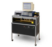
YTV B2 AOI
Tabletop Automated Optical Inspection
- Quick Set-up
- Color Camera
- High Defect Coverage
- Low False Failure Rate
- Best Price Performance
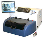 YESTech’s advanced Thin CameraT technology offers off-line tabletop PCB inspection with exceptional defect coverage. This table-top system inspects solder joints and verifies correct part assembly enabling users to improve quality and increase throughput.
Programming the B2 is fast and intuitive. Operators typically take less than 30 minutes to create a complete inspection program including solder inspection.
- Quick Set-up
- Mega-pixel Color Camera
- High Defect Coverage
- Low False Failure Rate
- Best Price Performance
YESTech’s advanced Thin Camera™ technology offers off-line tabletop PCB inspection with
exceptional defect coverage. This table-top system inspects solder joints and verifies
correct part assembly enabling users to improve quality and increase throughput.
Programming the B2 is fast and intuitive.
Operators typically take less than 30 minutes to create a complete inspection program
including solder inspection. The B2 utilizes a standard package library to simplify training and insure program portability across manufacturing lines. Programs created with the B2 are also compatible with YESTech’s complete line of AOI systems.
Newly available image processing technology integrates several techniques, including color, normalized correlation and rule-base algorithms, to provide complete inspection coverage with an extremely low false failure rate.
The B2 is equally effective for pre / post-reflow or even final assembly inspection. Remote programming maximizes machine utilization and real-time SPC monitoring provides a valuable yield enhancement solution.
Automated Inspection for:
- Solder & lead defects
- Component presence and position
- Correct part
- Polarity
- Through-hole parts
- Paste